I’ve seen lots of clones of the Philips Ambilight system that extend a TV picture out onto the surrounding walls by shining coloured LEDs out from the back of the TV. I wanted to do the same with my TV but all the clones out there seemed to be software based, requiring a PC to be producing the TV picture which they then grab frames from, analyse to get the light colours and drive the lights. My TV picture comes from MythTV, so I already have the PC running permanently, but I was worried that the extra load might cause problems when watching blu ray rips. I also wanted to have a lot of LEDs and I didn’t want the lag that is often seen between the TV picture and the LED output.
So I thought I’d try making a completely hardware based Ambilight clone that directly takes in a 1080p HDMI signal.
Click here to jump to the demo videos.
UPDATE: Version 2 is here
Specification
Here’s what I wanted it to do:
- Direct HDMI input
- Full frame rate 1920×1080 @ 60 Hz
- Up to 8 strips of WS2811 LEDs
- Up to a total of 256 LEDs, each able to set its colour independently from any arbitrary area of the picture
Multiplying these numbers showed that this would need to do a lot of work to keep up. That’s just over 124 million pixels per second, and with 256 independently controlled LEDs it will need to decide if a pixel needs to contribute to a particular LEDs colour nearly 32 billion times per second, and that’s before it does the maths to calculate the actual colour.
As that was way beyond any microcontroller’s capability and beyond most microprocessors I decided to use an FPGA, specifically a Xilinx Spartan-3E in the form of a Papilio One 250K board.
HDMI Receiver Board
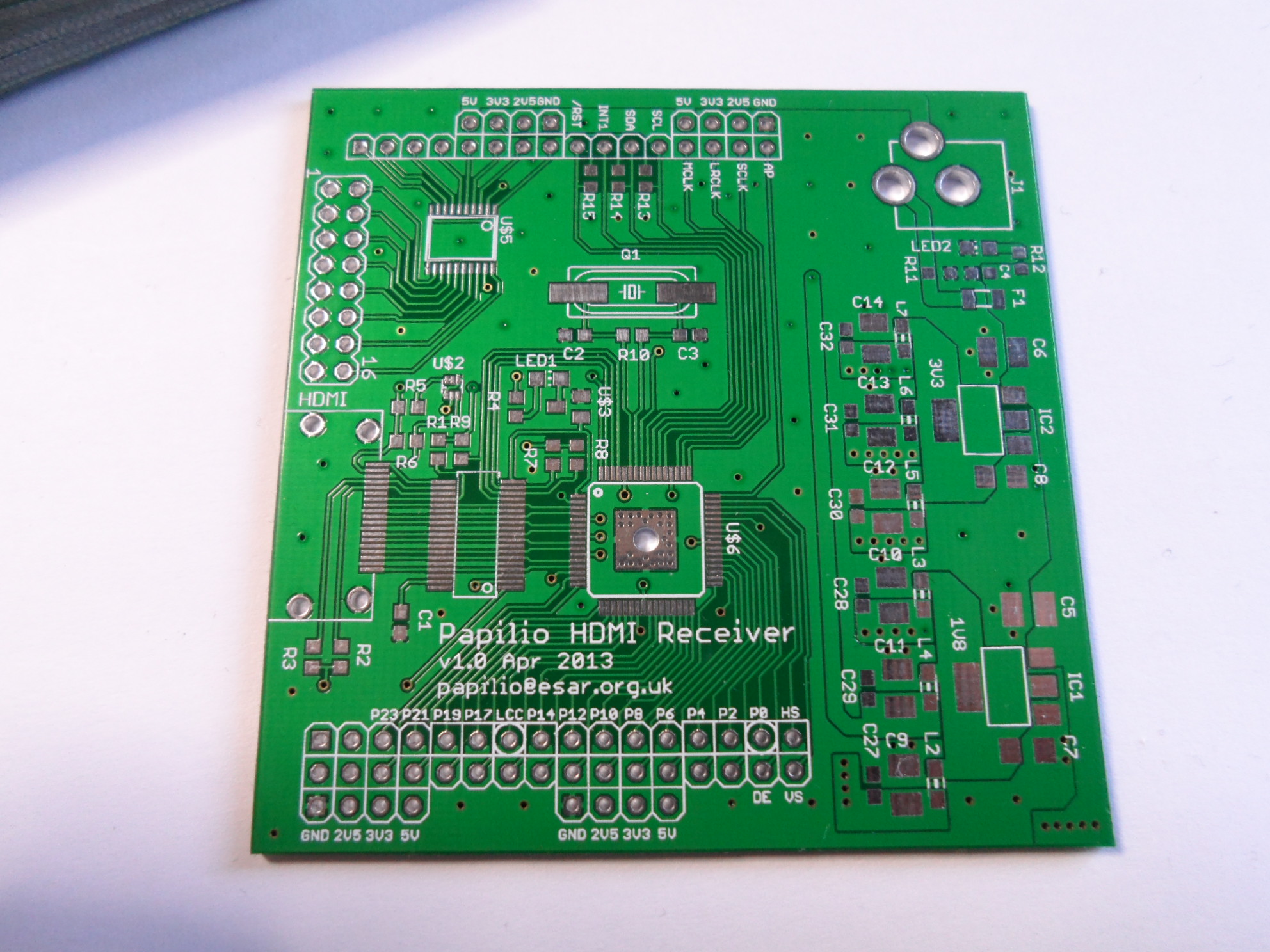
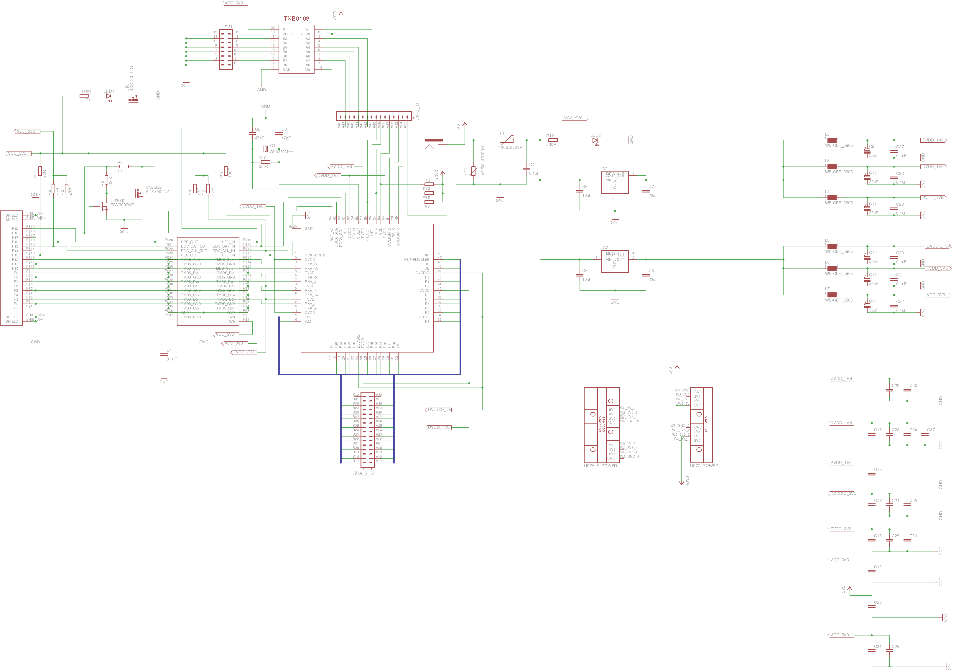
The first step was to create an HDMI receiver board for the Papilio and after a bit of research the ADV7611 from Analog Devices seemed to be a good (if quite expensive) chip to base it on. It’s a one chip solution to take in HDMI and output RGB pixel data on a 24-bit bus, apparently it will even handle HDCP protected content using built-in keys.
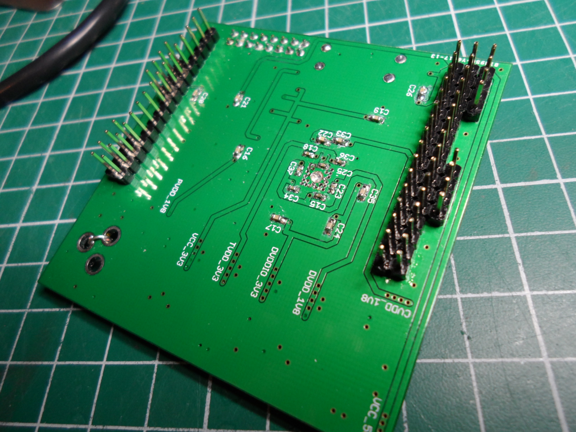
To make things easier Analog Devices have a Circuit Note titled ‘CN0282: USB Powered DVI/HDMI-to-VGA Converter (HDMI2VGA) with Audio Extraction‘ which is a complete design of a HDMI to VGA converter using this chip. I then just had to rip out all the parts of the design that I didn’t need and layout a board in Eagle, changing the ESD protection to a one chip solution stocked by Farnell and swaping the power supplies for linear regulators to save board space. I also added an eight channel 3.3V to 5V level shifter to drive the LED strips.
Once the board was laid out, I sent it off to Seeed Studio to be manufactured. One month and $25 later I received eleven copies of my board, ready to be populated.
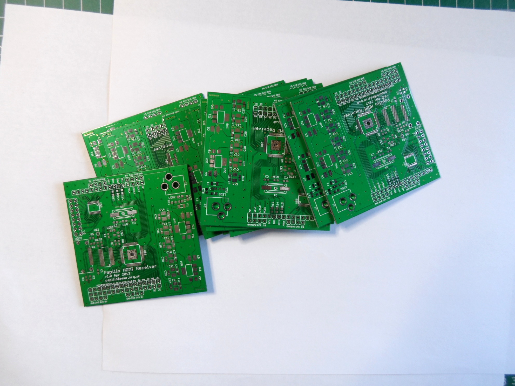
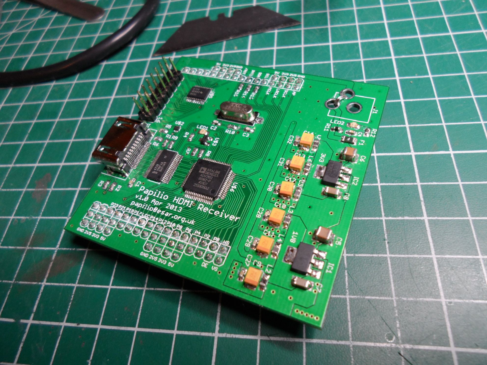
A couple of evenings with the soldering iron later and the board was ready for testing.
Testing The Board
Testing began the same way it does with everything else, set the bench supply to a low current limit, power up the board and check voltages at various points to make sure everything is behaving as expected and that no magic blue smoke is leaking out. This initial check passed and as the ADV7611 is controlled via I2C the next step was to connect it to a Bus Pirate and attempt to query the chips ID and version.
This second test didn’t go so well, I couldn’t get a reliable answer from the chip and when it did respond it wasn’t with the values I expected. My first suspicion was that the pad on the bottom of the chip wasn’t soldered properly, as it’s the only ground for the whole chip it’s a critical connection and trying to solder it through a 2mm hole in the PCB is not easy. Luckily after applying more heat and more solder my suspicion was confirmed and the chip started talking.
With the chip responding it was time to try and get it to produce some output, this thing has a lot of registers to configure it, so this part involved a lot of time trawling through the datasheet, but eventually I figured out how to get it into ‘free run’ mode which is where it outputs a blue screen with internally generated video timing when it has no input. With this mode enabled I was able to see the horizontal and vertical video sync output signals and that the blue pins on the data bus were active.
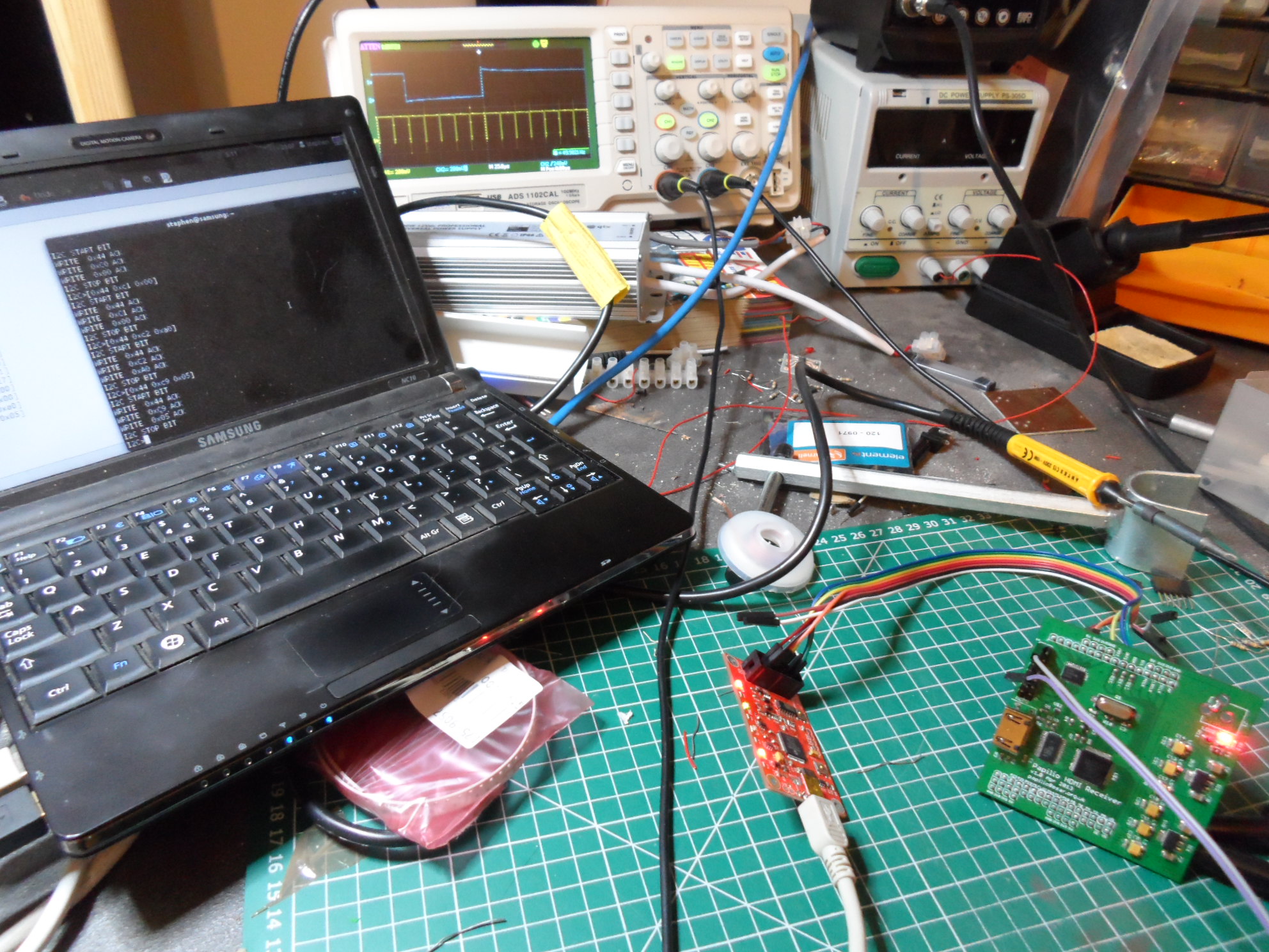
The final and hardest part of testing the board was getting the HDMI input working. This involves setting a whole load more registers and setting the contents of the EDID EEPROM. Eventually after wading through the datasheet and various application notes I got it working, and with a Raspberry Pi connected as the video source I was able to change the colour of the screen on the Rasberry Pi and see the changes reflected on the output bus of the ADV7611.
FPGA Design
The top level of the design for the FPGA contains three main components, an AVR compatible CPU and a UART, both from the CPU_LECTURE project at opencores.org, and an ambilight component, which is where the real work happens. I won’t spend any time describing the AVR and UART as they’re really well documented by their author. I’m using them to allow the ambilight component to be configured via the USB serial port on the Papilio and to configure the ADV7611 chip via I2C (which needs around 300 I2C writes to setup).
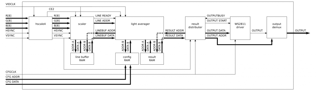
The block digram above gives an overview of the components and connections within the main ambilight component. On the far left are the inputs VIDCLK, R, G, B, HSYNC and VSYNC which all come directly from the pins of the ADV7611. Also on the left are CFGCLK, CFG_ADDR and CFG_DATA which connect the ambilight’s configuration RAM to the AVR CPU. On the far right is the OUTPUT bus that connects to the output pins that drive the LED strips.
The are two clock domains in this design. VIDCLK is the pixel clock from the ADV7611 (called LLC or Line Locked Clock in the datasheet) and at 1080p60 is running at 165Mhz. This clock is used by the hscale4, scaler and light averager components as well as both ports of the line buffer RAM, one port of the config RAM and one port of the result RAM. CFGCLK is generated in the FPGA and runs at 16MHz, it is used by all of the other components. The config and result dual port RAMs connect the clock domains.
FPGA Design: hscale4
The incoming video data is connected to the hscale4 component. This simply divides the horizontal resolution of the video by four. This is done to give the following components more than one clock cycle to preform the work for each pixel. I wasn’t able to get the remaining components to operate in a single clock cycle and still meet timing for 165MHz.
The internals of hscale4 are pretty simple, the 8-bit R, G and B buses go to separate adder trees which accumulate four pixels of data, at which point the bottom two bits are discarded to divide the result by four, producing a value that is the average of the last four pixels.
Additionally the HSYNC and VSYNC signals are delayed to account for the pipeline depth of hscale4 and two clock enable signals are generated CE2 and CE4, which respectively enable on every 2nd or 4th clock. CE4 isn’t actually used anywhere any more.
FPGA Design: scaler
The next stop is the scaler component which divides both the horizontal and vertical resolution of the video, dividing the horizontal by 8 and the vertical by 32, which with the scaling already performed by hscale4, results in scaling both dimensions by 32. This reduces the incoming 1920×1080 video to 60×34.
The operation of the scaler is similar to that of hscale4, except because it’s scaling in two dimensions it has to remember the accumulated count for each horizontal pixel to allow it to add to their counts for each of the 32 rows that are being averaged together. This is what the line buffer RAM is used for. It is sized to accommodate two lines of scaled video so that the scaler can be scaling incoming video into one line while the light averager component can be reading from the previously scaled line.
The scaler has four clock cycles of VIDCLK to process each incoming pixel from hscale4. It takes one clock cycle to read the previous accumulated value from the line buffer RAM and a second to pass that value through the adder trees and back into the RAM. Additionally, the scaler component is effectively running at half the frequency of VIDCLK by using the CE2 clock enable signal, which makes it much easier to get the design to meet timing.
As well as writing scaled video data to the line buffer RAM, the scaler also generates a LINE_READY signal to indicate that the next line is ready for processing and LINE_ADDR which is the line number that is ready.
FPGA Design: light averager
The light averager is the central component that does the real work, it reads light definitions from the config RAM, compares them against pixel data in the line buffer RAM and accumulates each light’s colour in the result RAM.
The config RAM is treated as an array of 32-bit values, one for each of the 256 light definitions. Those 32-bit values are broken down as follows:
- 6-bits: xmin (0 – 63)
- 6-bits: xmax (0 – 63)
- 6-bits: ymin (0 – 63)
- 6-bits: ymax (0 – 63)
- 4-bits: divisor shift count (0 – 15, divide by 1 – 32768)
- 3-bits: output pin (0 – 7)
- 1-bit: unused
So each light defines a rectangle of the scaled video that should be averaged to produce its final colour. To keep things simple the area of the rectangle must be a power of two so that the division that completes the average calculation can be performed by a right shift.
The result RAM is 72 bits wide, with one 72-bit value for each light. These values are broken down as:
- 21-bits: R (0 – 0x1FFFFF)
- 21-bits: G (0 – 0x1FFFFF)
- 21-bits: B (0 – 0x1FFFFF)
- 3-bits: output pin (0 – 7)
- 6-bits: unused
The R, G and B values in the result RAM are large enough to accumulate the value of every pixel on the screen, however the final step performs the right shift to divide them and calculate the average, and the next component will only read the lower 8-bits of each value. The light averager also copies the output pin address from the config RAM to the result RAM so that there are only two components that need access to the config RAM (the CPU and the light averager).
The operation of the light averager is controlled by one 16-bit counter. The bits of the counter are then used to create the following control signals, from least significant bit upwards:
- 1-bit: WRITE_CYCLE
- 8-bits: LIGHT_ADDR
- 6-bits: XPOS
- 1-bit OVERFLOW
These control signals are combined with the line address (or YPOS) that comes from the scaler so that for every pixel of video data, it iterates through every light definition, and for every light definition there is both a read and a write cycle.
The light averager always reads the current accumulated value for every pixel for every light, and it always passes this value and the new pixel value through the adder trees. It then generates a WRITE_ENABLE signal by comparing the current XPOS and YPOS against the light definition, and this WRITE_ENABLE signal controls whether the new value is actually written to the result RAM, and therefore whether the colour of the pixel contributes to the light’s final colour.
This is all performed in a three stage pipeline to keep the combinatorial delays low enough to meet timing.
FPGA Design: result distributor
The result distributor waits for the vertical blanking period to start, at which point it iterates through each of the 256 entries in the result RAM. It uses the output pin address to control the output demux and passes the final RGB colour of each light to the WS2811 driver.
It must complete its iteration through the results before the vertical blanking period ends as the light averager will start overwriting the result data as soon as the next frame begins.
FPGA Design: WS2811 driver
The WS2811 driver takes the parallel RGB data from its input and converts it to WS2811 compatible serial output. It uses the 16MHz clock, taking four clocks to output each bit. Over the four clock period it outputs ‘1110’ for a ‘1’ and ‘1000’ for a ‘0’, which keeps things nice and simple and is close enough to the correct timing to work.
Firmware
The firmware serves three purposes, first it initialises the ADV7611 chip via I2C, second it populates the config RAM with the light definitions, and finally it provides an interactive interface via a serial terminal to allow the user to modify the light definitions, query the resulting light colours, and read and write on the I2C bus to play around with the config of the ADV7611.
Currently the interactive interface supports the following commands:
- Set light definition:
- S light_number x_min x_max y_min y_max divisor_shift_count
- Get light definition:
- G light_number
- Get light result:
- R light_number
- Initialise I2C:
- I I
- Configure ADV7611 (from compiled in table of I2C address/values):
- I C
- I2C Write:
- I W address value
- I2C Read:
- I R address
Test Videos
Below are videos of the first time the whole system was tested. For this test my MythTV frontend PC is mirroring the display so that the same output goes to both the HDMI and DVI outputs. The HDMI connection goes to the TV, the DVI goes through a DVI to HDMI cable and into the HDMI Light. Both outputs are 1920×1080, the first test is 50Hz (UK TV), the second is at 24Hz (Blu Ray Rip).
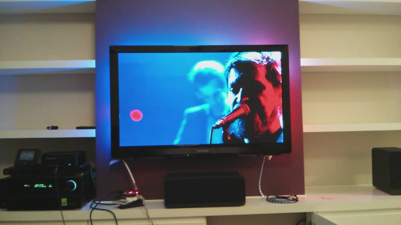
For this test there is a single strip of LEDs draped over the back of the TV and there are 32 LEDs on the left edge, 57 LEDs on the top edge and 32 LEDs on the right edge, for a total of 121 LEDs.
As you can see the alignment between the LEDs and the TV is slightly off. Also, I believe the LEDs are updating just ahead of the TV, so I may have to introduce some artificial lag to match the TVs internal processing delays.
Known Issues
For anyone attempting to recreate any of this, here’s a list of known issues:
- The power jack on the HDMI receiver board is connected wrong, don’t populate it, instead add a link to bridge the 5V from the Papilio board to the HDMI receiver 5V rail.
- The 3.3V to 5V level shifter IC is not suitable for the job as it’s not capable of driving a signal down any significant length of wire.
- LLC (VIDCLK) isn’t connected to an FPGA pin that’s on a clock net so the external pin mapping and board layout needs rearranging to be able to get a more optimal routing within the FPGA. However, it does seem to work fine as it is with CLOCK_DEDICATED_ROUTE set to FALSE for that pin.
- Added 10/11/2014: The pull-up resistors for the DDC and CEC lines were incorrect and prevented the EDID from being retrieved, this has now been fixed in the eagle files. The changes were:
- R1: 27R -> 27K
- R2: 47R -> 1K5
- R3: 47R -> 1K5
- R7: 47R -> 47K
- R8: 47R -> 47K
- R9: 100R -> 100K
Files
UPDATE 14/12/2014: There’s now a version 2 so these links are out of date.
Browse: repo
Download HDMI receiver board schematic: png
Download HDMI receiver board gerbers: zip
Really ? No Comments? can’t believe…
where to buy? 🙂 i’m no hardware hacker but this looks amazing.
This is great, thanks!
Awesome project! I ordered your board at a pcb fab and I will start building the device as soon as I get my ADV7611 chips. I hope I can contribute some improvements on github.
Cool! Let me know if you have any problems getting it up and running
I forked the repo at https://github.com/twasiluk/hdmilight and fixed the DC jack. If anyone wants to contribute feel free to send me a pull request.
Hi !
Very good device ! In the market just http://lightpack.tv/ can do the same effect, but it has a limited input ( only work on computer control )
I think many people is looking for it,.
Why don’t you put it in a product and sell it to the world.
Because not everyone is hardware engineer.
Thanks, but I just do this for fun. Finding out how to make it work is fun, turning it in to a product and dealing with customers is definitely not fun.
Lightberry is even better 🙂
Tom / esar,
Have you though of adding a ADV7630 to the schematic? Its an HDMI splitter, so the board could have an HDMI-In and HDMI-Out for a true “Pass-though” solution.
Here is the Datasheet:
http://www.analog.com/static/imported-files/data_sheets/ADV7630.pdf
Now that is an excellent idea, if Tom (or anyone else) hasn’t already done it, then when I get a chance to return to the project I’ll definitely look into this.
Tom,
Do you have any of the PCB you had fabricated left over? Also, what do you think of adding the ADV7630 (HDMI splitter) to the schematic / pcb design? I would do it myself, but I am terrible at PCB layout 😉
In case anyone wants to know, the cost of this project if you are starting from scratch is only about $208 (if you don’t already have a papilio one). This includes shipping and everything. I’ve got a complete BOM for Mouser which totals up to 53.80 w/ shipping if anyone is interested.
This is a great project! Thank you for the detailed description and thank you for publishing everything as open-source!
By the way: You have used the ADV7611BSWZ-P which cannot decode HDCP (labeled with -P). There is a version of the ADV7611 that can decode HDCP, but as far as I know it’s not easily available.
Interesting, thanks. Good job I never got around to trying to handle HDCP, I’d have spent ages thinking I just hadn’t configured the registers quite right!
I thought at the time that it was a bit strange that you could just put an encoder and decoder IC back to back and remove all of the encryption with almost no effort at all. Maybe you need to sign agreements to get hold of the HDCP versions, so that they know you won’t do that?
I’ve had a look at this board http://www.digilentinc.com/Products/Detail.cfm?NavPath=2,400,836&Prod=ATLYS which just has a Spartan 6 and a TMDS141RHAR HDMI Hider in between the Spartan and the HDMI port which seems slightly cheaper than the ADV7611.
Could this be a cheaper alternative that could be implemented say on a combined Spartan3 and TMDS141 instead then maybe code the spartan to do some HDCP (probably unlikely)?
While I’m hesitant to say it’s impossible, I think it’s at least impractical. The problem is that the TMDS141RHAR is really just a buffer, it’s not doing any processing at all, which leaves the FPGA to do everything itself. Somehow the FPGA has to receive and decode four separate channels that are each running at around 1.5Gbit/s.
I’ve seen it done on the sending side, specifically this guy just about manages it on a Spartan-6:
http://hamsterworks.co.nz/mediawiki/index.php/Spartan_6_1080p
However, I’ve never seen it done on the receiving side.
What the ADV7611 does is convert the four really fast serial lines that carry the signal on the HDMI cable to one slow (~150MHz) but wide (24 bit) parallel bus. This then makes things relatively easy for the FPGA as the maximum clock rate is a small fraction of the rate needed for the raw serial data.
That is interesting. So for all intense and purpose the Digilent board with it’s two HDMI input is really only a gimic intended to show off 720p and nothing higher.
That is a shame.
Do you know of a Buffer or decoded chip that will do what the ADV7611 does but not decode or mangle the data stream, so that if it’s HDCP it just passes it through. I would like to look at making a media converter, Something like justaddpower.com but not with that price tag.
If your aim is to feed one source to multiple displays then I don’t think pass-through of HDCP will be enough. Each display will need the video to have been encrypted with that display’s individual key. So the video must be separately encrypted for each display.
I think the only way to do this is either to create something that uses the leaked master key, which could then never be sold, or to get a license and your own key, which I’m guessing would be very expensive.
Yeah, I agree. My cunning plan stumpted at the gate.
I suspect that the reason justaddpower is so expensive is the royalties paid to get HDCP keys and lock things down.
Thanks for your advise. Neat project BTW.
I’ve just found this product.
http://en.honestar.com/product/datasheet/ITE/IT6604%20Datasheet%20v0%207%20.pdf
Only $5 a piece and seems to do HDCP
Now I wonder if it’s an “Approved item”? Probably not.
Nice find! It doesn’t look like it’s carried by any of the main distributors and the documentation on the registers is hard to find, but I might buy a couple anyway. It looks like it’s part of a whole family of chips, including receivers, transmitters and splitters.
Of course, it may turn out to be the same as the ADV7611, where all of the documentation says it handles HDCP with internal keys, but in reality you need a license to get hold of the version with HDCP. I still can’t find where it’s documented that there even is a non-HDCP version, let alone that that’s the only one you can buy.
I would suspect that it does have HDCP, but it’s the leaked one and that it’s now locked out by the newer media.
isn’t Alibaba a main distributer :p
The other thing I was thinking the other night is how do HDCP compliant HDMI splitter work, specially multi chipped verion? They have got to have a Reciever and then a set of transmitters. Is the lines between reciever and transmitter un encrypted, it would have to be because each TV would have it’s own set of keys.
Maybe that’s another way to get a HDMI through capability with HDCP.
I’m trying to implement the VHDL under ISE, but it’s giving me the following errors:
ERROR:NgdBuild:604 – logical block ‘ambilight_inst/conf’ with type ‘configRam’
could not be resolved. A pin name misspelling can cause this, a missing edif
or ngc file, case mismatch between the block name and the edif or ngc file
name, or the misspelling of a type name. Symbol ‘configRam’ is not supported
in target ‘spartan6’.
ERROR:NgdBuild:604 – logical block ‘ambilight_inst/scaler/line_buffer’ with type
‘line_buffer_ram’ could not be resolved […]
ERROR:NgdBuild:604 – logical block ‘ambilight_inst/lightAverager/resultBuffer’
with type ‘resultRam’ could not be resolved […]
Any ideas how to resolve that? I’m using ISE 14.7 and a Spartan6 (Papilio Pro), but the same happens for ‘spartan3e’.
Earlier it complained about missing ngc files for those 3 elements, so I generated them from the projects in fpga\ipcore_dir.
BTW I bought a ADV7611 with HDCP, have not signed/licenced anything. I can test it out once I manage to generate a bitstream. I guess you can buy the HDCP versions in low quantities without a hassle, but if you need to manufacture a product for sale then you probably need to get certified (i.e. pay a lot of $$$).
You should just need to regenerate the IP cores for the block RAMs. These are the steps I just took to test this:
1) clone a refresh copy of the repo
2) Open fpga/hdmilight.xise in Xilinx ISE 14.4 (lin64)
3) In the Hierarchy pane on the left, expand the tree and select the conf, line_buffer and resultBuffer entries one by one, and for each one run the Regenerate Core process in the pane below
4) Select the HdmilightTop item in the Hierarchy Pane
5) Run the Generate Programming File process
This results in a bit file being successfully generated. I believe the dangling pin warnings are expected, though it’s been a while so I’m not 100% sure. Interestingly they don’t happen on my current working copy which targets the Spartan-6 on the Papilio Pro (I’m planning on moving to the Papilio Pro for the extra block RAMs so that I can implement some delay on the output to get it exactly in sync with my TV).
At some point I may try replacing the IP core block RAMs with generic VHDL which would make the regeneration unnecessary and make things more portable.
btw, in case you find it useful, I’ve put my (completely untested) UCF file for the papilio pro here: http://pastebin.com/SXNZQybx.
Thanks for the detailed instructions! I managed to get a bitstream so I’m on my way to test out the wing. I wonder how many soldering issues I will find 🙂
Cool, good luck!
Great work!
I’m new on FPGA and I saw Makefile s into the project folder. Are you using Linux? or running make files over ISE Command Prompt? What it your OS suggestion for FPGA design?
Thank you
Yes, I use Linux for almost all of my work. For this project I create the bit file from within the Xlilinx ISE GUI and then run make from the Linux command line to do the rest. The makefiles should work fine on Windows too if Cygwin or similar is installed (though I haven’t tried them).
Personally I prefer working on Linux, but there are pro’s and con’s to both Windows and Linux, and I’ve used both over the years. Once you’ve got a working tool chain it doesn’t really matter, it’s really down to which ever environment you’re most comfortable with.
I will try to compile it over Cygwin and I will keep you informed.
I saw a lot of blogger using Linux for FPGA, I will follow your way 🙂
Thank you very much for this clear answer.
Hi Again,
I tested the MakeFile over Cygwin but didn’t compile firmware because of no avr-gcc implementation on cygwin. Checked some blogs, they are saying completely hopeless for avr over cygwin.
Another reason to starting Linux based FGPA development.
Thanks for the update.
It may be possible to use WinAVR or the gcc behind AVR Studio and just use make from Cygwin, but if you’re happy using Linux then that’s the easiest option as everything should just work.
I just finished to install ISE on Ubuntu. It was huge job for me because Xilinx ISE is not supporting free Linux distros,(only costly RedHat and Suse)
I have still some Licence Manager problems but not a big issue.
Anyway, I just tried the compile your Make file under Ubuntu and received following error from avr-gcc compiler. Do you know the reason?
In file included from main.c:30:0:
config_hdmi.h:31:27: error: variable ‘g_configTable’ must be const in order to be put into read-only section by means of ‘__attribute__((progmem))’
static struct ConfigTable g_configTable[] PROGMEM =
^
In file included from main.c:31:0:
config_lights.h:38:22: error: variable ‘g_lightTable’ must be const in order to be put into read-only section by means of ‘__attribute__((progmem))’
static unsigned long g_lightTable[] PROGMEM =
Thank you
It may be the version of avr-gcc you have installed is a bit stricter than the one I’ve been using. Can you let me know what version you’re using (I think “avr-gcc -v” should tell you)? I’ll try the same version and see if I get the same issue.
It’ll probably just need that line changing to:
static const struct ConfigTable g_configTable[] PROGMEM =
I’ve been able to recreate this with avr-gcc 4.8 and I’ve committed a fix. Pull the latest version from the repo and it should build ok.
This is amazing. I want to buy one, nobody sells it?
Hi esar,
I want to extract audio stream from this HDMI receiver ADV7611. But I dont know how to interface ADV7611. I have read the Circuit notes, but don’t know how to start with it.
Can you please tell me how to start with it. Waiting for your response….
Thanks,
Ajmeri Jaimin
I’ve not tried to do anything with audio so I can’t really help. From a quick look at the datasheet and user guide it looks like the ADV7611 can output either I2S or SPDIF on the AP pin, and that it outputs I2S by default.
I’d guess it just starts outputting audio data on the AP pin whenever there is valid HDMI input.
Hi, I would like to suggest to kickstart the HDMI light ! You could get in contact with lightpack guys or do it alone.
It would need to include the Papilio FPGA equivalent and the hdmi receiver board in a package.
Xilinx is known to give special prices to kickstarter campaigns.
Todo :
– Add passthrought at 1080p60hz with 3d support (splitter IC)
– Add support for 8 ws2812b lanes (ie floor, ceiling …)
– Add more zones ( Scaler: 4 and 16 instead of 8 and 32) (will the XC3S250E support it?)
– configuration for zone-to-leds config (support up to 144led/m)
– import/export .cfg file (usb disk like interface?)
– have a audio in port for mood lightning.
– add Brightness, Contrast, Saturation preprocessing
– add LUT adjustment
– design enclosure
It would kickstart in no time !
Adding HDCP would be great, not sure if aliexpress can provide HDCP splitter chip for mass production …
I’d pledge for one (no leds), best price range would be 59-99$.
Think about it.
As I’ve mentioned before further up the comments, I’ve got zero interest in turning this into a commercial product. That’s far too much like real work for my liking. However, everything necessary is here, so anyone else is free to try.
Thanks for the feature suggestions though, coincidentally I’d been working on some of this over the weekend. Here are my comments on the individual points:
– Add passthrought at 1080p60hz with 3d support (splitter IC)
This should be fairly straightforward using a splitter IC, if I ever make a revision to the PCB then I’ll almost certainly do this.
– Add support for 8 ws2812b lanes (ie floor, ceiling …)
This is already in the current version, it supports up to 256 LEDs, each of which can be arbitrarily assigned to one of eight outputs.
– Add more zones ( Scaler: 4 and 16 instead of 8 and 32) (will the XC3S250E support it?)
The XC3S250E can’t do this, the problem is actually the small amount of RAM available. I needed to get all of the configuration for each LED packed into 72 bits or less so that it could all be available at once using a single block RAM. This meant 6 bits each for the 4 coordinates that define the area to average and therefore a max value for 63 for each coordinate.
I’ve now moved to the Papilio Pro for my current work-in-progress version, which has a Spartan-6 LX9 with much more memory. This should mean that it will be possible to use two block RAMs for the LED config, allowing for 144 bits of config per LED and much higher resolution.
I’ll add this one to my todo list.
– configuration for zone-to-leds config (support up to 144led/m)
I don’t think I understand what you mean
– import/export .cfg file (usb disk like interface?)
That would be a nice interface, but probably quite a bit of work to implement, so personally I’m unlikely to do this as I wouldn’t get much gain from the time spent on it.
– have a audio in port for mood lightning.
I have considered this briefly and it’s one of the reasons that I connected the audio output of the HDMI chip to the FPGA, but other than that I’ve never done any actual work towards making it happen
– add Brightness, Contrast, Saturation preprocessing
I’m actually working on this one right now. As you can see in the photo at the top of the page, the wall above my TV is purple, and as a result I’m implementing per strip colour correction that will account for the wall colour.
This is being implemented using a 3×3 transformation matrix on the RGB output and will allow all sorts of transformations, including brightness, contrast, saturation and even remapping of the colour channels or complete colour space conversion
– add LUT adjustment
I’m not sure what you mean by this. LUT = Look Up Table?
– design enclosure
It’s not likely that I’ll ever get around to doing this.
There are 3 major différent led strip configuration : 30 60 144 les per meter.
As for controlling more led and having a dynamic control to change configuration without recompilling the whole thing, I would recommend to add an additionnel chip. Could be a AVR or ARM M0-M3. The FPGA would output the color values of the zones to the chip. This chip could process those values according to the configuration of the LEDs and control them. It could serve as memory to dump colors from the FPGA as soon as a zone is processed. Those chips have USB chips that could provide simple serial prompt to configure the different tv/led configurations and control brightness(easy to prog a gui). Also say you have a 60inch tv with 1024 LEDs, it would smooth the colors values of one zone over multiple LEDs. This could be a cheaper alternative to larger FPGA. Some arm are SoC that include wireless. An IR or android interface would be possible. This add-on chip could add lots of expansion options.
Thanks for your hard work! I don’t have the skills to assemble a PCB, any one has one for sale?
After looking around, I found HUE lights that could be controlled by wifi. http://www.limitlessled.com/dev/
So a ARM chip could add interesting mood lights.
Perhaps sound could be use to modulate the leds, hier pitch = less smoothing and pulsing color quickly (ie bright blue/blue); lower bass = more intense light and smooth the color longer (fading to black would be slower) …
Thanks
Eventually I do plan to integrate this with the rest of my home automation stuff, partly so I can turn it on and off without getting off of the sofa, but also so I can use the strips as general lighting.
I’ve had a bit of a marathon session this weekend and now have a whole collection of new features working…
Before there were a fixed set of 256 light definitions, each of which specified a screen area to average and an output channel to select the destination strip.
Now there are 256 screen area definitions, 8 (soon to be 64) colour transformation matrices and 8 gamma correction tables.
Each output channel now has a table that defines up to 512 LEDs (for a total of 4096 LEDs), where each entry in the table specifies which screen area definition to take the colour from, which colour transformation matrix to use, and which gamma correction table to use.
The colour matrices can also be used to set the strips to fixed colours and intensities independently from the HDMI signal by setting the main coefficients to all zeros and then adding a fixed offset.
I’ve also added configurable output delay so that the output can be precisely synchronised with the screen. The output can be delayed by up to 7 frames, in steps of 1 microsecond.
All I’ve got to do now is work out how I’ve managed to stop it working at full 1080p resolution.
Terrific project! I am curious about one thing though, there’s going to be a mismatch between the color gamut of the TV and the LEDs, are you transforming your color spaces via CIE 1931 to compensate for that? Or are your LEDs “close enough”?
Most of the time the difference isn’t too noticeable, there are the odd occasions though when the TV is showing a slightly dull red and the LEDs are pumping out full on primary red, the same happens with some blues, I’ve never noticed it with greens
I’ve been assuming this is just a problem with gamma, but maybe it’s actually what you’re describing with the different colour space that can’t represent some of the colours.
I’m actually close to completing version 2, which adds colour transformation matrices and gamma correction tables. From a quick scan of the wikipedia article on CIE 1931 it looks like it might be possible to do the transform (or a close approximation) with a simple matrix.